Huawei made big news this week.
They basically laid out their plan for closing the semiconductor performance gap with Nvidia (and the West). Without being too reliant on EUV in particular.
So, it is a pretty political story.
But, more importantly, Huawei laid out an approach that will (if successful) fundamentally change chip design. It’s a new circuit architecture.
Everyone is writing about this right now. And serious engineers are wondering if Huawei can pull this off.
I won’t go into the technical details (not my expertise). I’ll give you my simplistic explanation. And then I’ll jump to 3 things I think everyone is getting wrong.
LogicFolding: Get Ready for 3D Circuitry
Huawei has described their LogicFolding architecture as a shift from geometric scaling to time-based scaling (tau scaling). And they argue this new architecture will unlock all types of improvements in performance, including greater compute density, better power efficiency, and higher clock speed.
Here’s my simple explanation.
Huawei is designing quasi-3D circuits. Instead of flat chips, think of quasi-3D chips with more vertical layers and connectivity.
Within these circuits, the connections (all the way to the transistor and gate level) will use both horizontal and vertical routing. And this means lots more compute in the same physical area (i.e., higher compute density). That is how they get to the claim that these will be equivalent to 1.4nm chips by 2031.
Going to 3D circuitry shortens the wires connecting all the transistors. Instead of wires (connections, not really wires) going longer and longer-distances horizontally, the key ones can just go short distances vertically.
That decrease in wire length (again, not really wires) means reducing resistance and capacitance. This is part of how you decrease signal propagation delay (τ), which is the foundation of their tau scaling approach. With less resistance and capacitance, everything is faster and with less energy required. That’s also how you get the higher clock speed and other cited benefits.
So, 3D circuitry and the scaling law are about increasing compute density and compressing signal propagation delay.
Nvidia is Still the Leader in Chip Performance. But Huawei is Moving up Fast in Architecture and Interconnect.
For those of you who follow me, this approach should sound familiar.
I’ve been writing a lot about Huawei’s new AI Data Centers, which have a somewhat similar approach. The new data centers (CloudMatrix, SuperPoD, SuperCluster) are also using new architecture plus faster interconnect to improve the overall performance (with less powerful chips).
Central to this is Huawei’s UnifiedBus.
We heard a lot about UnifiedBus with the Atlas 950 SuperPoD data center that Huawei showcased at Mobile World Congress in January. Here’s my article on that.
It turns out if you’re going to get 8,192 NPUs together into a new integrated compute architecture, you need super-fast interconnect.
The UnifiedBus interconnect, which leverages all-optical links, is how Huawei solved the 8,192 NPU connection problem.
FYI: Here’s what the Atlas 950 SuperPod looks like:
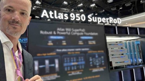
That’s the SuperPod, which has 8,192 NPUs in 160 cabinets. In the upcoming SuperCluster, they are connecting +500,000 NPUs.
***
Ok. That’s a simplistic explanation for the new architecture and scaling law.
In Part 2, I go into how they are doing this.
-Jeff
*Disclosure: AsiaTech Services, LLC has had a paid commercial relationship with Huawei within the past 12 months. This article received no financial sponsorship or backing.*
——–
Related articles:
- How Generative AI Services Are Disrupting Platform Business Models (2 of 2) (Tech Strategy – Daily Article)
- The Winners and Losers in ChatGPT (Tech Strategy – Daily Article)
- Why ChatGPT and Generative AI Are a Mortal Threat to Disney, Netflix and Most Hollywood Studios (Tech Strategy – Podcast 150)
From the Concept Library, concepts for this article are:
- Semiconductors
From the Company Library, companies for this article are:
- Huawei
- HiSilicon
———
I am a consultant & keynote speaker on how to increase digital growth and strengthen digital AI moats.
I am the founder of TechMoat Consulting, a consulting firm specialized in increasing digital growth and strengthening digital AI moats. Get in contact here.
I write (a lot) about digital growth and digital AI strategy (3 best selling books, +2.9M followers on LinkedIn). There is a free book and email newsletter below.
My Moats and Marathons book series is a framework for building and measuring competitive advantages in digital businesses.
This content (articles, podcasts, website info) is not investment, legal or tax advice. The information and opinions from me and any guests may be incorrect. The numbers and information may be wrong. The views expressed may no longer be relevant or accurate. This is not investment advice. Investing is risky. Do your own research.