There is a lot of discussion about Huawei’s new architecture. Especially around the technical aspects.
This article what I think people are missing.
**Sponsored: I was compensated by Huawei for sharing my thoughts about this event / announcement. Opinions expressed are my own.
1. The New Architecture Shifts the Bottleneck from Transistor Physics to Interconnect Physics
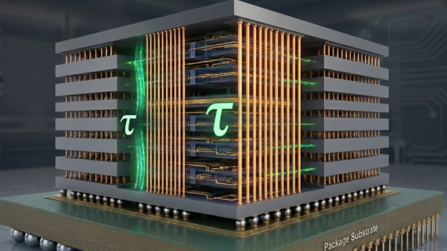
The standard industry focus (Moore’s Law) optimizes the transistor gate. However, in modern sub-7nm regimes, the other performance problem is the RC delay (the resistance-capacitance time constant, which is represented by the Greek letter τ). As the microscopic copper or ruthenium wires get thinner, resistance spikes exponentially.
With LogicFolding, Huawei is shifting the 2D layout of logic blocks into pseudo-3D or highly compressed configurations
They are treating the chip not as a collection of switches, but as a complex network of highways where shortening the physical length of the wires does more to lower tau than a smaller node would.
Pseudo-3D circuitry is based on architecture innovation and fast interconnect. The interconnect aspect is going to be really complicated and interesting.
2. Huawei’s 381-Chip Variants Means This Is Already an Edge-First, Mobile-Tested Architecture
A big technical challenge everyone is pointing to is thermal crowding.
When you compress circuit layouts via layers to bypass geometric limitations, you fundamentally alter the thermal dissipation.
- In a standard flat chip, heat generation is proportional to surface area (A).
- In a layered architecture, power density per footprint area increases significantly, while the primary cooling path remains through the same flat 2D surface area at the top.
Stacked layers increase vertical thermal resistance, making heat extraction from deeper layers more challenging.
The 41% power efficiency boost Huawei has claimed is not just a benefit (which it is), it is also a mandatory survival threshold. The chip must run at lower operating voltages to prevent thermal runaway.
The 41% power efficiency boost Huawei has claimed is a significant advantage. And it also helps manage the increased thermal density of the folded architecture.
So, can they do it?
In her keynote, HiSilicon President He Tingbo mentioned that Huawei has already mass-produced 381 chip variants using Tau Scaling principles over the last six years.
That got my attention.
That means this architecture was prototyped and tested on edge devices long before being scaled up (happening this year). Edge devices are small. And they have incredibly strict thermal and physical boundaries.
So, I think they have been testing this architecture across hundreds of lower-risk, low-power edge chips. I’m thinking they have already mapped out the defect rates, parasitics, and mathematical modeling for LogicFolding.
They are launching this architecture at scale with the Fall 2026 Kirin smartphone SoC. So, I’m thinking they already have this solved.
We’ll see.
3. Huawei’s New Architecture Will Change the Dynamics of Semiconductor Competition
Competition in semiconductors has been a lot about network effects at Nvidia and economies of scale (i.e., big spending) in fabs.
But Huawei’s new architecture will shift this dynamic
Semiconductor competition will go from mostly a game of Big, Specialized Equipment Buying
To a game that is also focused on:
- Multi-Level Co-Design
- Physical Architecture Innovation
- Algorithmic Routing
What does that mean?
Both advanced EUV geometric shrinking and 3D architecture can be used to improve performance.
Competition will shift towards having the best optimization for of a more complex architecture.
Basically, watch for engineers spending a lot more time on the increasingly complex architecture, advanced geometric mathematics and routing algorithms. In addition to the standard focus on materials science.
For a better explanation, see this paper by He Tingbo.
——-
I am a consultant & keynote speaker on how to increase digital growth and strengthen digital AI moats.
This content (articles, podcasts, website info) is not investment, legal or tax advice. The information and opinions from me and any guests may be incorrect. The numbers and information may be wrong. The views expressed may no longer be relevant or accurate. This is not investment advice. Investing is risky. Do your own research.